Introduction to TEM microscope
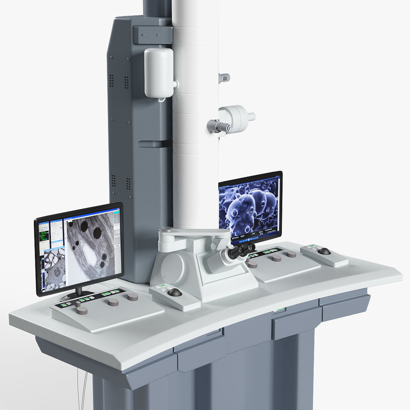
TEM microscope, commonly known as TEM, is a critical tool in the world of nanotechnology. This specialized microscope uses a beam of electrons to create highly detailed images of tiny structures. In comparison to light microscopes, TEM offers a much higher resolution. It can magnify objects over two million times, providing insights into the morphological features and composition of specimens.
Developed in the early 20th century, TEM microscope uses the principles discovered by scientists like Louis de Broglie. These principles helped understand the wave nature of electrons. The advancements led to the first TEM prototype by Ernst Ruska and Max Knoll in 1931. Later improvements by Ernst Ruska with Siemens resulted in the TEM we know today.
How does TEM microscope work? It beams electrons through a thin sample. As electrons interact with the specimen, they create an image with fine detail. The equipment includes key components like the electron gun, condenser lenses, and image recording systems. Featured with a vacuum system, TEM captures the electron image on a fluorescent screen or digitally.
TEM microscope plays a vital role in nanotechnology research. It has made possible detailed studies of structures as small as viruses and nanoparticles. In TEM’s three main systems, each plays a part. The electron gun generates electrons. The image-producing system magnifies the image. Lastly, the image recording system captures the data.
Whether it’s biology, materials science, or electronics, TEM helps scientists explore and understand the tiniest particles. Its powerful magnification has brought forward a new frontier in research, driving forward significant advancements in numerous fields.
Historical Evolution of TEM Microscopes
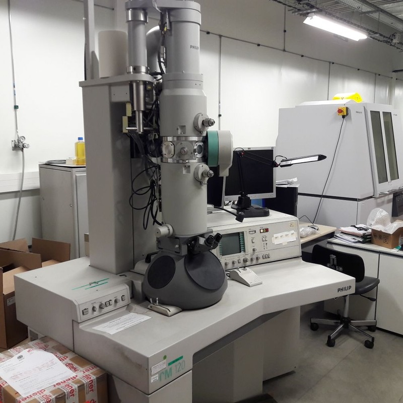
The journey of TEM microscopes begins with Louis de Broglie’s theory in the 1920s. His findings on the wave-like nature of electrons set the stage for electron microscopy. In 1931, scientists Ernst Ruska and Max Knoll built the first TEM prototype. This event marked a crucial point in scientific imaging.
TEM technology saw rapid improvements after its inception. Siemens worked with Ernst Ruska in the early 1930s. Together, they enhanced the TEM, boosting its imaging capabilities. This collaboration led to the production of the first commercially viable TEM.
Over the years, TEM has evolved with technological growth. Its key components have seen refinements. Electron guns now use lanthanum hexaboride for sharper, focused beams of electrons. Advancements in lens technology have improved magnification and resolution.
Digital advancements have transformed TEM’s image recording system. Gone are the days of just fluorescent screens. Now, digital cameras capture highly detailed images. These can be analyzed and shared more easily than ever before.
In summary, TEM’s historical evolution is a tale of continuous refinement. From its conceptualization to modern tweaks, each step has pushed the boundaries. Today’s TEM microscopes are far more powerful than their early counterparts. They serve as a window to the minuscule wonders of nanotechnology.
Key Components of a TEM Microscope
A Transmission Electron Microscope (TEM) is an intricate device composed of several critical components that work together to produce detailed images at the nanoscale. Understanding each part’s function helps grasp how TEMs advance the field of nanotechnology. Here are the primary components:
- Electron Gun: This part generates the electrons needed to create images. It usually contains a tungsten filament or a lanthanum hexaboride rod. These elements heat up to release electrons.
- Condenser Lenses: These lenses focus the beam of electrons onto the specimen. A TEM often uses a two-lens system for better control over beam size and intensity.
- Specimen Stage: A platform where the sample is placed. It can move to allow electrons to interact with different parts of the specimen.
- Objective Lenses: Positioned close to the specimen, these lenses form the initial magnified image. They have a short focal length to capture fine details.
- Projector Lenses: These further magnify the image formed by the objective lenses. Their arrangement allows for a wide range of magnification levels.
- Fluorescent Screen: This screen makes the electron image visible to the human eye. It glows when struck by electrons.
- Digital Camera: Modern TEMs are equipped with digital cameras that capture the image for computer analysis. This allows for detailed examination and storage.
- Vacuum System: It maintains a vacuum within the microscope. This is crucial, as air molecules can scatter electrons and blur the image.
Each component’s precise design and operation are the heartbeat of a TEM microscope. They enable scientists to peer into the nano-world and uncover its secrets, driving forward research and innovation in countless fields.
Operating Principles of TEM Microscopy
To understand the advanced work TEM microscopes do in nanotech, it’s helpful to know how they operate. Let’s break down the operating principles into simple, bite-sized points:
- Electron Beam: A TEM microscope uses electrons, not light, to form images. Electrons can show much finer detail because they have shorter wavelengths.
- Magnification: Once electrons pass through a sample, magnetic lenses magnify the image. Different lenses work together to greatly enhance size.
- Sample Interaction: Electrons interact with the sample, scattering in various ways. This depends on the sample’s density and composition.
- Image Formation: As electrons scatter, an image begins to form. It shows different parts of a sample in different shades, based on how they interact with electrons.
- Vacuum Environment: All this happens in a vacuum. Why a vacuum? It prevents air from scattering the electrons, which keeps the image clear.
- Digital Capture: In the end, a camera or screen captures the image. Now, scientists can see and study tiny structures in great detail.
These principles enable TEM microscopes to provide incredibly detailed views of the nanoworld. They are essential for advancements in various fields of nanotechnology.
Sample Preparation Techniques for TEM Analysis
Preparing samples for TEM analysis is a delicate process that is crucial for achieving accurate and informative images. Here are the steps typically involved in preparing samples for TEM:
- Fixation: Samples are first fixed using chemical agents like glutaraldehyde or osmium tetroxide. This preserves the specimen’s structure.
- Dehydration: After fixation, organic solvents such as ethanol are used to dehydrate the specimen fully.
- Embedding: The sample is then embedded in a resin to make it firm. This aids in cutting ultra-thin sections.
- Sectioning: Using an ultramicrotome, very thin slices of the specimen are cut, usually between 20 to 100 nanometers in thickness.
- Staining: The sections are then stained with heavy metals like lead citrate or uranyl acetate. This enhances contrast by scattering electrons at different rates.
- Mounting: Finally, the stained sections are mounted onto grids to be inserted into the TEM for imaging.
- Freeze-fracturing: For some samples, a technique called freeze-fracturing is used. It involves freezing the specimen and then breaking it to reveal internal structures.
The success of TEM imaging largely depends on these sample preparation steps. Each step must be performed with precision to avoid artifacts and ensure the true representation of the sample’s nanostructures.
TEM’s Role in Nanotechnology Advancements
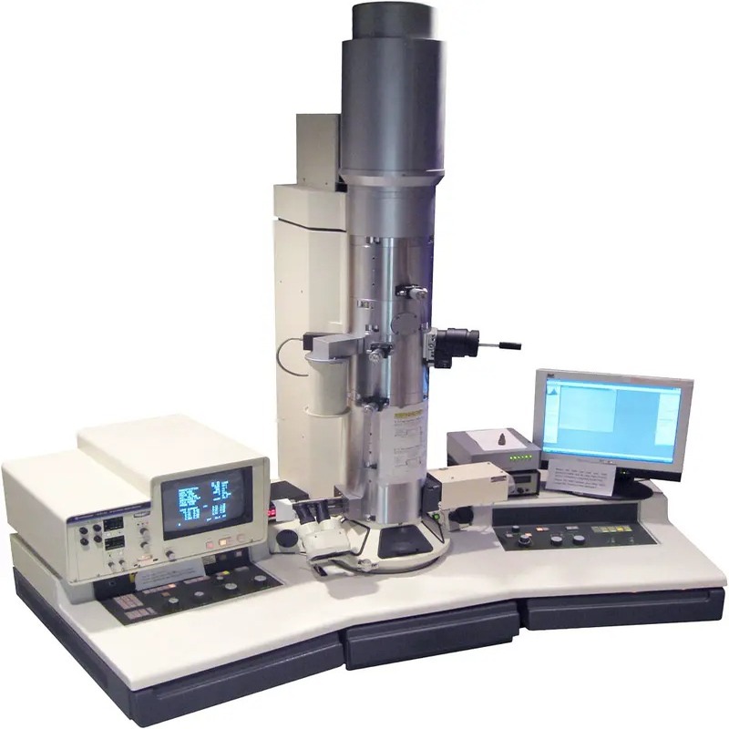
The role of Transmission Electron Microscopy (TEM) in nanotechnology is groundbreaking. This powerful tool has drastically changed how we understand and manipulate materials at the nanoscale.
- Visualizing Nanostructures: TEM’s ability to magnify objects over two million times allows for clear visualization of nanostructures. Scientists can see atoms and molecules in high resolution.
- Material Characterization: Researchers use TEM to analyze material properties. This includes size, shape, and distribution of nanomaterials. Such details are vital for developing new nanotech products.
- Nanodevice Engineering: TEM aids in the design of nanodevices. By observing how materials behave at the nano level, engineers can create more efficient devices.
- Biomedical Applications: In medicine, TEM helps study cell structures, viruses, and nanomedicines. This leads to better disease understanding and potential cures.
- Nanoparticle Research: The microscope can analyze nanoparticles in detail. Understanding their interaction with environments promotes safe and effective application.
- Quality Control: TEM ensures quality in nanomanufacturing. It checks for defects and impurities that could affect performance.
- Academic Research: Beyond practical applications, TEM is a cornerstone in nanoscience education. It trains the next generation of researchers in nanotech.
In short, TEM drives advancements in nanotechnology. It gives researchers and engineers the power to explore, innovate, and create on a scale once unimaginable.
Advantages and Limitations of TEM in Research
When assessing the impact of Transmission Electron Microscopy (TEM) in research, it’s important to consider both its advantages and limitations.
Advantages of TEM in Research
- High Magnification: TEM is renowned for its ability to magnify specimens over two million times.
- High Resolution: It provides unparalleled detail, revealing the structure of materials at an atomic level.
- Material Analysis: TEM’s detailed imaging supports in-depth analysis of material properties.
- Diverse Applications: It has applications across various fields, from biology and materials science to nanotechnology.
- Improved Imaging: Digital cameras and advanced software have increased TEM’s imaging capabilities.
- Structural Insights: With TEM, researchers gain insight into the internal structure of nano-sized objects.
Limitations of TEM in Research
- Sample Preparation: Preparing specimens is complex and time-consuming.
- Cost: TEM equipment and maintenance are costly.
- Size Constraints: Only thin, electron-transparent sections can be examined, limiting the range of samples.
- Monochromatic Images: Images are greyscale, which can make interpretation challenging without additional processing.
- Equipment Sensitivity: TEMs are sensitive to vibrations and require controlled environments.
- Operational Complexity: Proper operation requires in-depth knowledge and training.
By understanding these advantages and limitations, researchers can make informed decisions about when to employ TEM microscopes in their studies. While the instrument has some drawbacks, its benefits are substantial, making it an indispensable tool in the advancement of nanotechnology and many other research domains.
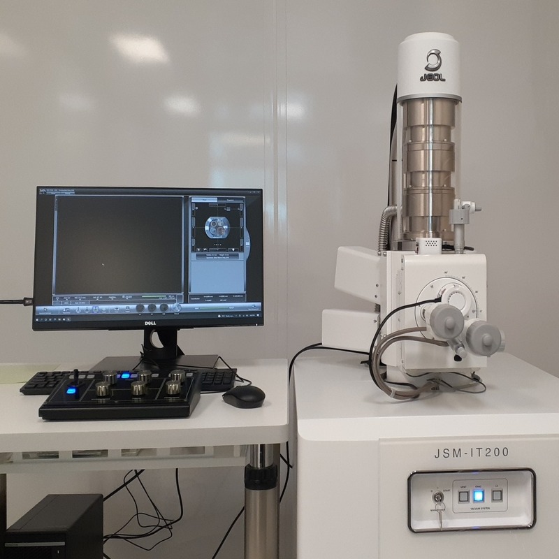
Future Directions for TEM in Nanoscience
As we gaze into the future of nanoscience, TEM microscopes are set to play a pivotal role. Innovations in TEM technology will likely focus on further enhancing resolution and versatility, making it an even more powerful tool for research and development.
Improving Resolution
Scientists are continually pushing the boundaries of TEM to achieve even higher resolutions. Advancements could provide unprecedented views of atomic structures, potentially revolutionizing materials science and nanotechnology.
Versatility and Adaptability
Future TEMs may offer greater adaptability for a variety of sample types. This would significantly expand the range of nanoscience applications, from environmental monitoring to space exploration materials.
Automation and Artificial Intelligence
Integrating AI with TEM operations could streamline the imaging process. This integration would enable quicker, more precise analysis and could revolutionize the way researchers study nanomaterials.
In-situ Experimentation
Developments in in-situ TEM techniques will allow scientists to observe reactions and processes in real-time. This could lead to breakthroughs in understanding how nanomaterials form and interact.
Enhancing Accessibility
Reducing the cost and complexity of TEM equipment is another key direction. More affordable and user-friendly TEMs could democratize access, spurring innovation across diverse fields and regions.
Multidisciplinary Collaboration
Stronger collaboration between various scientific disciplines could foster new TEM applications. By combining insights from physics, chemistry, and biology, TEM could unlock secrets of the nanoworld currently beyond our grasp.
TEM microscopes have evolved from simple imaging devices to complex instruments that shape our nanoscale understanding. Looking forward, these microscopes will continue to be at the nanotechnology frontier, driving new discoveries and innovations.
